


Jaideep Saraswat, Nikhil Mall
Introduction
India’s renewable energy journey has accelerated rapidly over the past decade, elevating the nation from a modest solar capacity of 3.74 GW in 2014 to an impressive 123 GW by August 2025. With 18.6 GW added in just the first half of 2025, India has solidified its position as the world’s second-largest solar market. While this growth is crucial for achieving the national target of 500 GW of renewable capacity by 2030, it brings into focus an essential question: are we ensuring that the installed capacity is translating into actual generation efficiency? Solar photovoltaic modules form the core of every installation and represent one of the most critical cost components. If these modules suffer from hidden defects, the long-term performance of solar plants is compromised. This is where Electroluminescence (EL) testing emerges as a transformative quality assurance tool.
EL testing is a non-destructive diagnostic technique that reveals internal defects in solar modules that cannot be detected through visual inspections or standard electrical tests. When a forward bias is applied to the solar module, it behaves like a light-emitting diode and radiates light in the infrared spectrum. Since this emission is invisible to the naked eye, a specialised infrared-sensitive camera is used to capture the image. The resulting EL image acts like an X-ray of the module, showcasing defects such as microcracks, inactive regions, shunts, and degradation patterns. The precision of EL testing makes it one of the most trusted methods for evaluating module quality, offering accuracy levels close to 99 percent in identifying even minute anomalies that could lead to major performance losses over time.
Why EL Testing Matters
As the solar industry matures, the focus is shifting from rapid capacity deployment to long-term asset performance. Even minor defects that may be electrically inactive during a module’s early years can propagate over time, leading to severe energy yield losses, diode activation, or hotspot formation. EL testing helps identify these defects early in the manufacturing, installation, or operational lifecycle, enabling stakeholders to take corrective action. It not only strengthens quality assurance but also plays a pivotal role in protecting investments, verifying manufacturer claims, and ensuring performance guarantees. With the rise in warranty disputes and insurance claims worldwide, EL testing has become essential for ensuring transparency, accountability, and the long-term sustainability of the solar ecosystem.
Where EL Testing is Used Across the Solar Value Chain
EL testing is strategically integrated across various stages of the solar value chain. In research and development, it is used to evaluate new materials, cell architectures, and manufacturing innovations. During the manufacturing process, it is used after cell production, stringing, and lamination to screen defects that could affect module integrity. Early-stage EL imaging allows manufacturers to detect cracks or soldering issues before lamination, enabling timely corrections and reducing scrap rates. In the field, EL testing is now an important tool for performance audits, predictive maintenance, and degradation assessment. Developers and asset operators are increasingly using portable EL devices and drone-based systems to monitor large-scale installations. The test is also critical for certification processes and warranty verification, offering third-party validation of module integrity.
How EL Testing is Performed
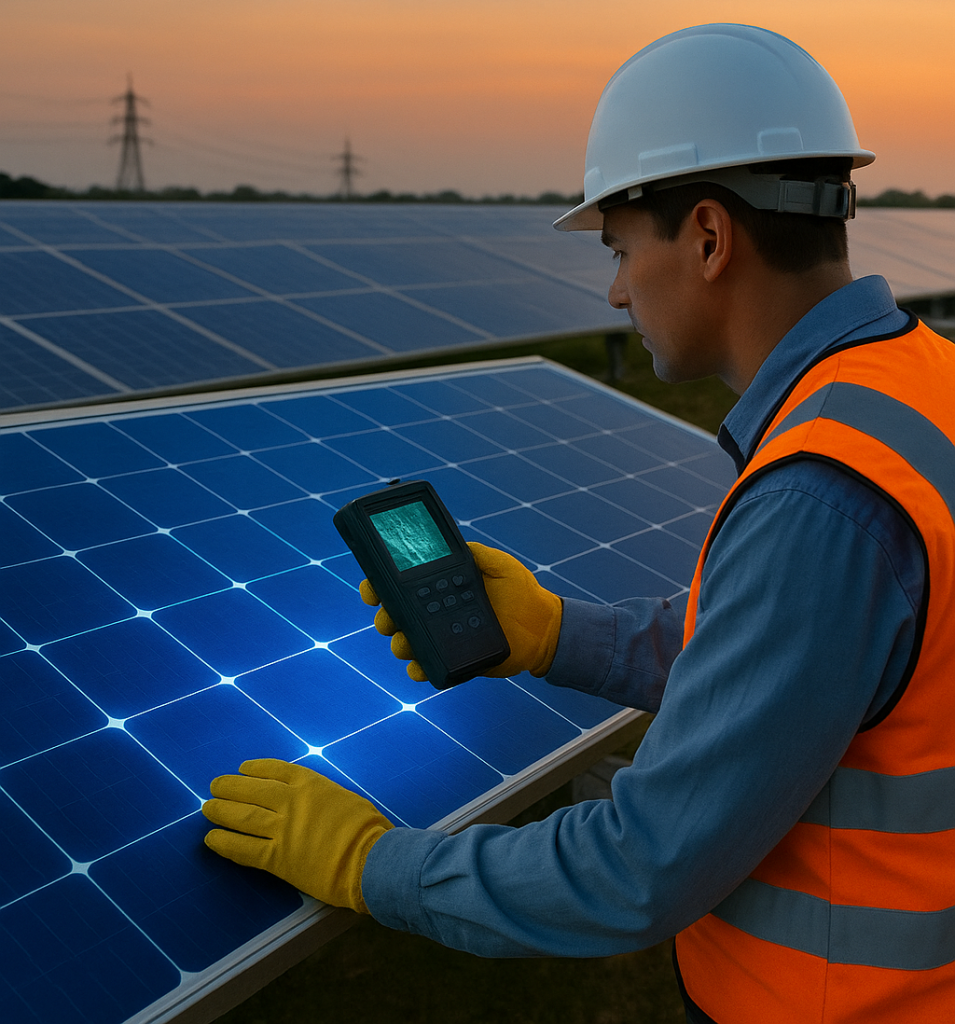
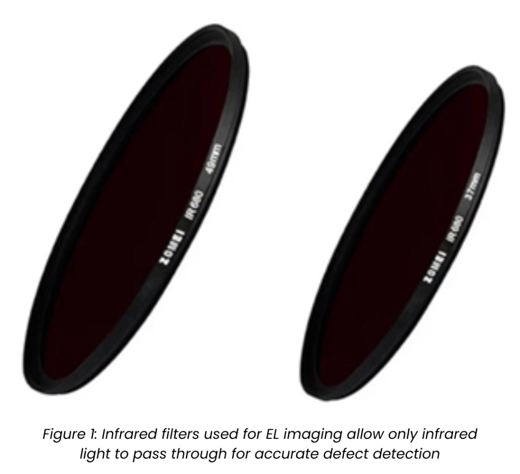
Conducting EL testing does not always require expensive laboratory setups. With a modified digital camera that can detect infrared radiation, along with an appropriate infrared pass filter (Figure 1), a user can capture EL images even at the field level. The test must be conducted in a dark environment or under a controlled hood to prevent light interference. It can be carried out even at the site where the modules are installed. A current source is used to forward bias the module. Typically, current levels between 70 percent to 120 percent of the module’s short circuit current are applied until a clear image is obtained. Care is taken to avoid overheating the module during this process. An EL image captured under these conditions reveals the electrical continuity and material uniformity of the cells.
Types of Defects Detected Using EL Testing
EL testing provides insight into cell health by analysing the intensity and uniformity of light emission in the captured images. Various defects produce characteristic patterns in these images, enabling precise identification of issues and informing appropriate corrective actions.
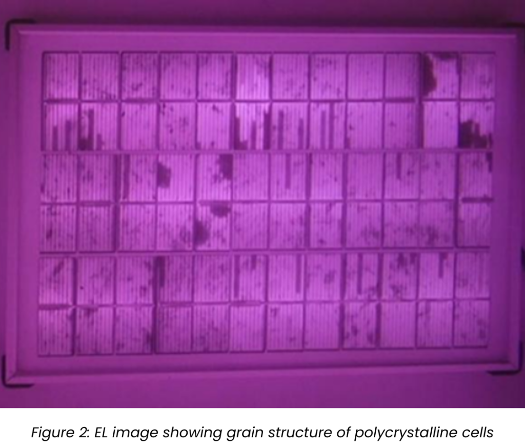
- Crystal Structure Differences: A monocrystalline module generally displays a uniform bright pattern due to its continuous crystal structure, while polycrystalline modules show varied patterns because of the grain boundaries inherent in their structure as seen in Figure 2.
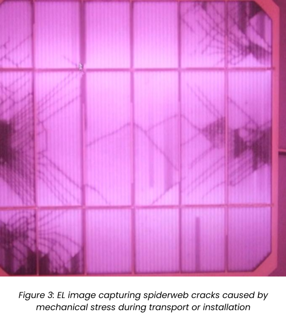
- Microcracks: One of the most common defects observed is microcracking (Figure 3), which often appears as dark, irregular lines. Microcracks are small fractures in the silicon wafer that may result from mechanical stress during manufacturing, transportation, or installation. These cracks can interrupt current flow, activate bypass diodes, and reduce module output.
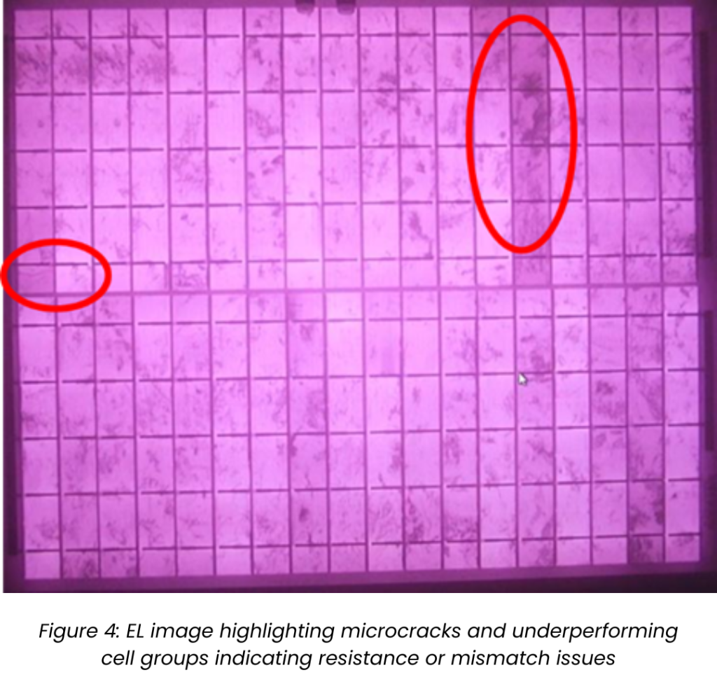
- Cell Performance Variation: Cells within a module may perform unevenly due to mismatched material properties, improper interconnections, or soldering issues. In EL images, this is observed as patches of lower brightness compared to neighboring cells as seen in Figure 4. This can lead to uneven power generation, potential localised heating, and reduced lifespan of affected strings.
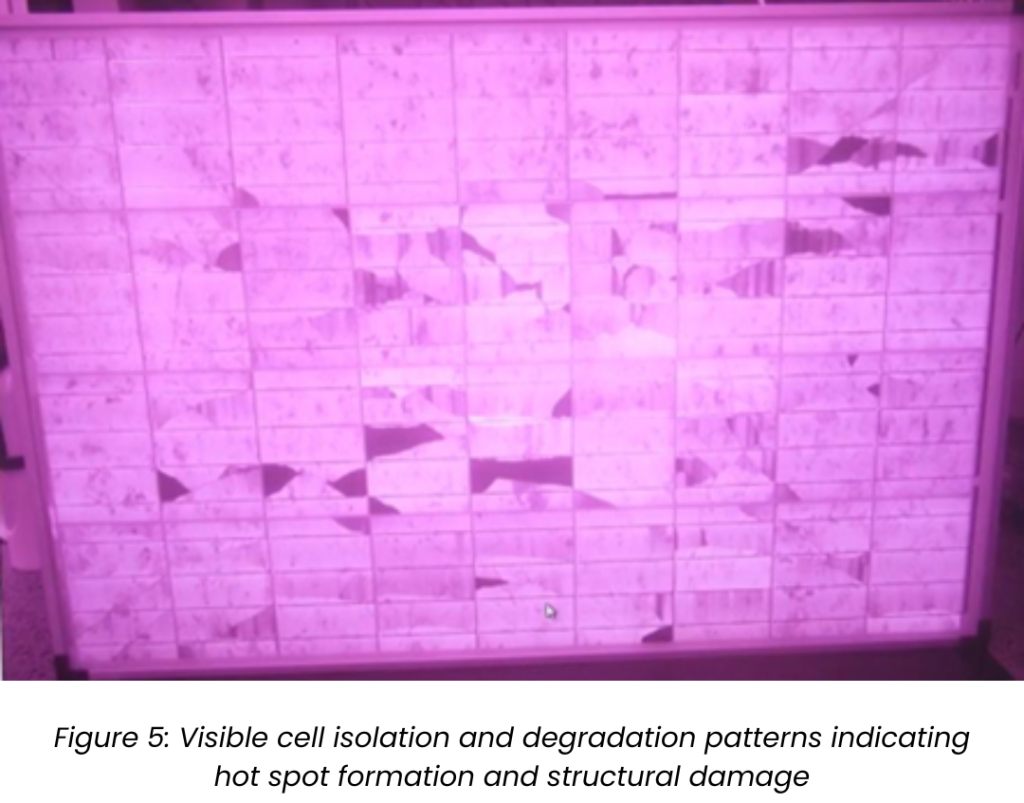
- Cell Isolation and Cracks: Some cracks can isolate portions of a cell entirely, preventing electrons from flowing through certain regions as seen in Figure 5. In EL images, these appear as dark patches surrounded by brighter, functional areas. Such defects can lead to significant power loss in the affected regions, formation of hotspots due to uneven current distribution, and faster degradation of the module if left unaddressed.
Other defects include Potential Induced Degradation (PID), which appears as dark spots at cell edges, dead cells that have lost electrical output, and diode failures that deactivate cell strings. Each of these defects, while sometimes invisible to the eye, has a direct impact on module efficiency, safety, and lifespan.
Conclusion
EL testing is far more than a diagnostic step; it is a strategic enabler of solar reliability and efficiency. Making EL image data available to consumers for each module can be a critical first step toward ensuring accountability and building trust in manufacturing quality. Even more compelling is the potential of capturing EL images directly at the deployment site, which offers real-world validation of module health and boosts consumer confidence.
To this end, Vasudha Foundation has been at the forefront of this effort, developing a dedicated deep learning model trained on over 25,00 labeled EL images to automatically identify and classify defects in solar modules deployed across rooftop and utility-scale installations. Beyond automated analysis, Vasudha Foundation is initiating on-ground validation surveys of solar rooftop plants deployed under the PM Surya Ghar: Muft Bijli Yojna (PMSGY), using random sampling to identify recurring defects and create a comprehensive solution framework. These initiatives not only improve defect detection and maintenance strategies but also enhance overall module performance, reliability, and longevity.
Explore our EL-defect detection model – a tool that identifies hidden defects in solar modules using EL images, shared openly so researchers and industry users can apply or build on it to enhance solar-panel reliability: https://github.com/ajay-VF/Solar-Defects
Stay tuned to this space for more updates!